|
Ball Valve American made ball valves by Valtorc International. American made, great pricing items in stock ready to ship.
|
 |
PCB Surface Processes |
 |
 |
 |
 |
| |
 Provides a solderable surface for Component assembly. Provides a solderable surface for Component assembly.
Protect Copper Surface from Oxidation.
Provide a surface appropriate for wear related parts.
Mixed Technology Board Designs
Solderable,SMT and Thru-hole
Wire Bondable
Contact Resistance
Co-Planar Surfaces
Compatability with variety of fluxes & paste
Cost effective
Environment
Electroless Nickle-Immersion Gold
Immersion Silver
Hot Air Solder Level
Organic Solderability Preservative
Electrolyte Nickel - Hard Gold
Electrolyte Nickel - Soft Gold
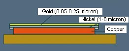
Electroless Nickel-Immersion Gold (ENIG)
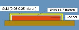 A two layer, gold over nickel, metallic surface finish plated onto the copper base by means of a chemical decomposition process. A two layer, gold over nickel, metallic surface finish plated onto the copper base by means of a chemical decomposition process.
| Advantage |
Disadvantage |
- Typical Thickness: 3-8 uin gold over 150-250 uin nickel
- Excellent Corrosion resistance
- Good for aluminium wire bonding
- Excellent flatness for fine-pitch technology
- Excellent Solderability
- Excellent shelf life(12 mo)
- Good surface contrast
- Good contact resistance
- High Aspect Ratio Capability
|
- Narrow process window
- Higher cost than HASL(1.5 to 2.0 times)
- Back pads: brittle solder joints
- Fatigue failures on large BGA packages
- Skip plate
- Extraneous nickel plating
- Solder mask capability with the nickel bath
|
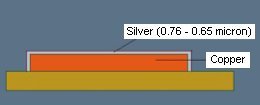 A co-deposit of silver and organics A co-deposit of silver and organics
| Advantage |
Disadvantage |
- Typical coating thickness: 5-25 uin
- Very good alternative to HASL (lead free)
- Similar cost to HASL
- Excellent Solderability,(Comparable to Solder)
- Excellent for fine pitch and BGA's technologies
- Holes Capability over 10:1 aspect ratio
- Press fit connector's capability
- Mulitple heat cycles during assembly process
- Reworkable product(at fabricator)
- Selective gold compatible
- Good Shelf life ,6 months to 12 months
- Conductive during PCB testing
- Low % Silver dissolved into silver joint
|
- No thermal cycle after Immersion
- Silver at the Fabricator
- Vias cap:UV curable only
- Handling
- Some resistance from the OEM to use
- Immersion Ag with press fit connectors
- Micro-void in the solder joints
- Also found on other surface finishes
- Discoloration due to reaction with sulfur in the air.
- (Does not impact solderability)
|
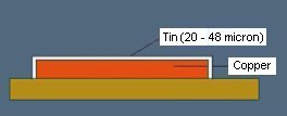
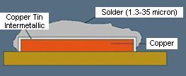 A molter solder immersion and hot air leveling(blasting) of surfaces and holes to provide a "pretinned" coating on exposed copper surfaces. A molter solder immersion and hot air leveling(blasting) of surfaces and holes to provide a "pretinned" coating on exposed copper surfaces.
| Advantage |
Disadvantage |
- Typical coating thickness specifications
- 100-1000 uin with average of 150-300 uin fine pitch
- 40-1000 uin on discrete pads with average 80 uin
- coverage on large surface (ground plane) 15-40 uin
- Excellent solder "Nothing solders better than solder"
- 20mils pitch capability; dependent on technology
- Board thickness up to 200 mils
- Panel size up to 24 x 28 inches
- One of the less expensive surface finish
- Good shelf life
|
- Uniformity of the coating
- Thermal shock
- Limited capability on high density borads
- Limited capacity to clear vias holes
(>6:1 aspect ratio)
- Difficulty to maintain hole size tolerance along
plated edges
- Difficulty to process thin material
- Require a different drill selection.
(Press fit connector dictate the drill)
- Process very dependant of the board technology
- Intermetallic layer grows with time and heat cycle
- Use of Lead
|
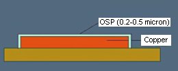 A water based Organic compound that selectively bonds with copper to provide an organomettalic layer that protects the copper for soldering A water based Organic compound that selectively bonds with copper to provide an organomettalic layer that protects the copper for soldering
| Advantage |
Disadvantage |
- Typical coating thickness: 8-20 uin
- Major advantage: Gold doesn't need to be protected
- The least expensive surface finish
- Reworkable
- Shelf life (6 months)
- New lead free OSP formulations available
|
- Difficult or impossible to inspect the final product
- Skip Plating
- Residue on Copper
- Coating thickness
- Difficult to soldermask via cap
- Electrical testing prior to coating
- Micro-void in the solder joints
- also found on other surface finishes
- Solder may not wet to corners of large SMT pads
(still good solder joint)
|
 A two layer,gold over nickel,metallic surface finish plated onto the copper base by means of a electrolytic deposition process. A two layer,gold over nickel,metallic surface finish plated onto the copper base by means of a electrolytic deposition process.
| Advantage |
Disadvantage |
- Good Connector. Typical thickness 30-50 uin
minimum gold (99.7 %)
over 150 uin minimum nickel
- Solderable Surface. Typical thickness 5-15 uin
minimum gold (99.7 %)
over 150 uin minimum nickel
- Excellent corrosion resistance
- 130 to 200 Knoop hardness
- Excellent wear resistance for surface rotary switches, on-off contacts,and edge connectors
- Excellent shell life
|
- Gold Distribution
- Throwing power in the holes
- The copper is exposed on the sides of the traces
- Porosity
- Difficulty to measure the true line width
- Soldermask adhesion on gold
|
 A co-deposit of Tin and organics A co-deposit of Tin and organics
| Advantage |
Disadvantage |
- Back Plane
- Press fit connectors Technology
- Reworkable
- Reworkable
|
- Soldermask compatability
- Thiourea (TU)
- High temperature of the Tin bath
- Process control:Solderability Test (Tin porosity)
- Intermetallic growth
- Solderabilty goes down significantly with each reflow cycle
- Unable to analyze chemistry directly
- solderabilty test(6-8 hr test)
|
Lead Free Compatible OSP
Enthone 106 HT Designed for Lead Free re-flow Profiles
Drop in Alternative to 106 AX (for Merix and CMS)
Survive Extra re-flow Cycle in a tin/lead Assembly
Easy Control Process
UIC Immersion Silver
Investigating to Reduce or Eliminate Tarnishing
Testing Planned
|
|
 |
|
 |
|